PCB Design Part 1
Disclaimer
This project includes images of assemblies that use third-party components from Phoenix Contact. The electronic housing shown in the images is a product of Phoenix Contact and is used here for reference and demonstration purposes only. All product names, logos, and brands are property of their respective owners.
PCB Design
We’ve arrived at the part I like the most: turning this:
Into this:
Below, I explain the step-by-step process I used and how I organized my ideas.
Case
The dimensions of all components together are 124x95mm. So, the first step now is to find a case.
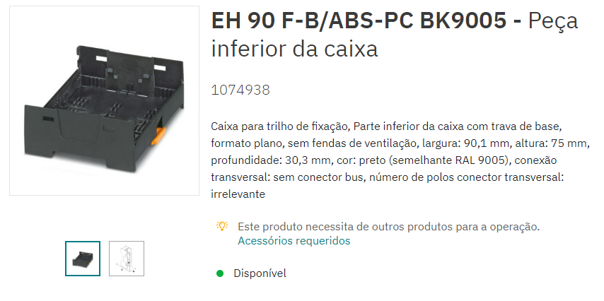
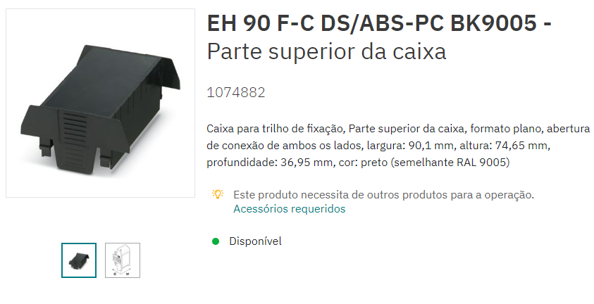
I won’t spend much time here; I’ll go straight to the Phoenix Contact website. They have excellent cases, at a higher price but still fair, and they are well-documented.
I’ll check out the cheaper cases.
The chosen ones:
Routing Start
The first thing to do is configure Kicad. I’ll set it up as follows:
- 4-layer PCB - It’s much easier to route a more complex board with 4 layers.
- Keep the mask green - it’s much cheaper and easier to find.
- Add track sizes (I like to use 0.2, 0.3, 0.5, and 1 mm).
- Add vias.
- Add the HTML Bom plugin.
The second step is to draw the board.
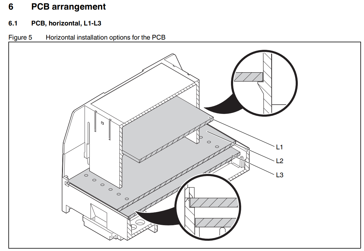
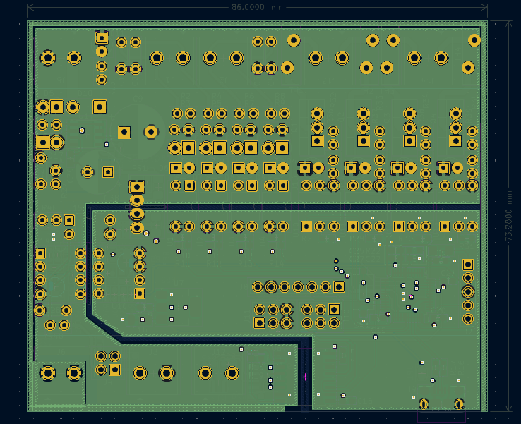
I’ll use the L2 board, which measures 73.2x86mm, with a 1mm clearance margin on each side.
It looks like this:
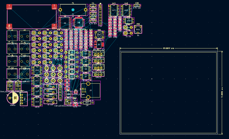
It’s already clear that it won’t fit, and as I route, I’ll need to redo some circuits. That’s because I really want to keep the case. Let’s continue the routing, and I’ll publish the changes.
You need to outline where the top part of the case will touch the PCB; I’ll show this drawing below.
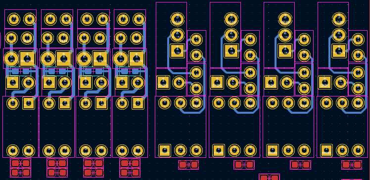
The first thing I do is route each subgroup of components: inputs, outputs, communication. Anything modular should be routed before combining the parts.
For example, the routing of the inputs and outputs after refining the component positioning quite a bit.
And so on, with all subcircuits. As they are routed and positioned, you start to see the best place for each one. You also see which circuits are the hardest to position within the chosen board dimensions. That’s how I identified the need to reduce resistors, change the 24V to 5V regulator circuit, and shrink the USB Type-B connector to fit everything on the board.
The final board is shaping up as shown below. On the left are the subcircuits for analog input and power supply. At the bottom is the isolated RS485 circuit.
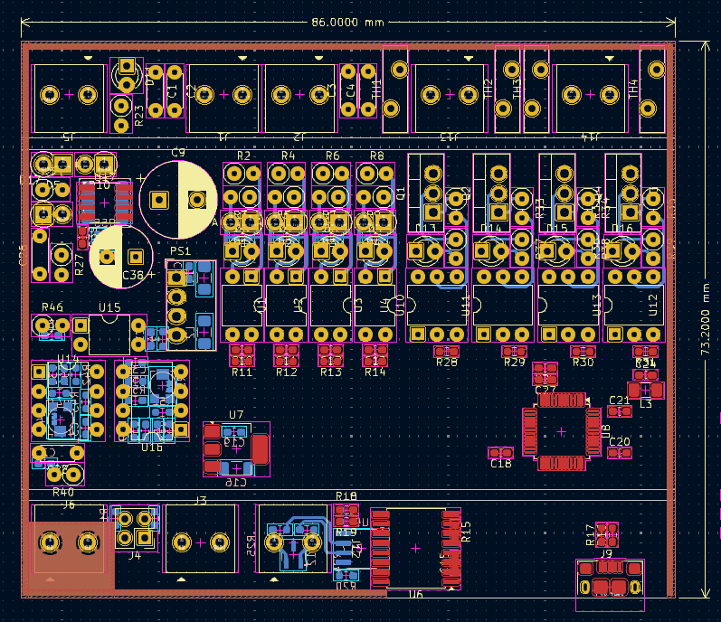
Some components are positioned but don’t have tracks yet because I already know I’ll be able to route them easily where they are. Right now, I’m more concerned with the general layout than the tracks.
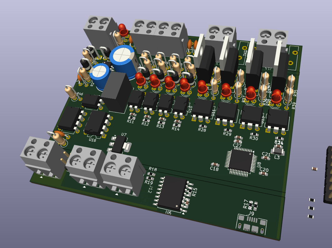
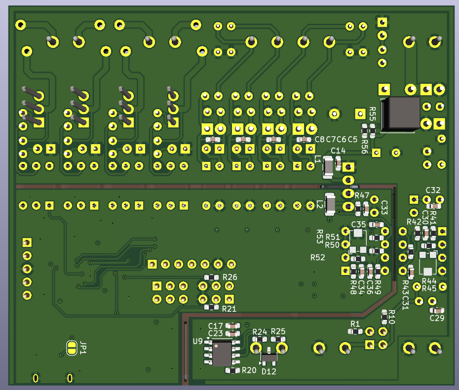
Notice that I outlined the area where the case lid touches the board and positioned the isolated components to achieve an almost rectangular isolation area. In the image below, I show how the isolated GND planes look:
Now I’ve reached a critical part: positioning the microcontroller.
When positioning the microcontroller, I prioritize the most critical signals (higher frequencies). They should have the shortest possible length, without vias and without interruptions in the ground plane to avoid creating an antenna effect and, more importantly, to ensure the signal is not degraded.
That’s why I placed the microcontroller as close as possible to the USB and RS485.
I started writing about the microcontroller signal routing process here, but the post became extensively long. Therefore, I will write a separate post about how I routed the microcontroller tracks and what to consider when routing higher frequency tracks.
Conclusion
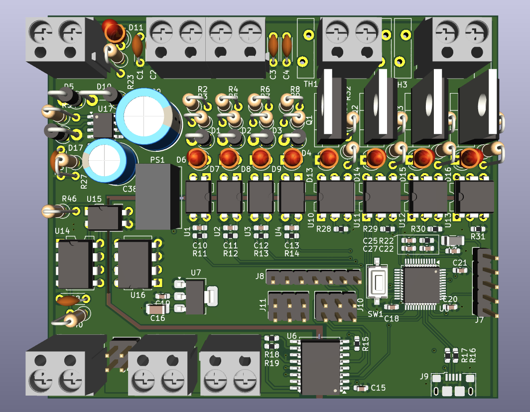
The final routed circuit:
Some directive texts for programming and usage are still missing, and I need to review some tracks. I like to do this a day or two after fully routing, like text proofreading. Once I’ve reviewed the board, I’ll generate the fabrication files and start the material procurement process.
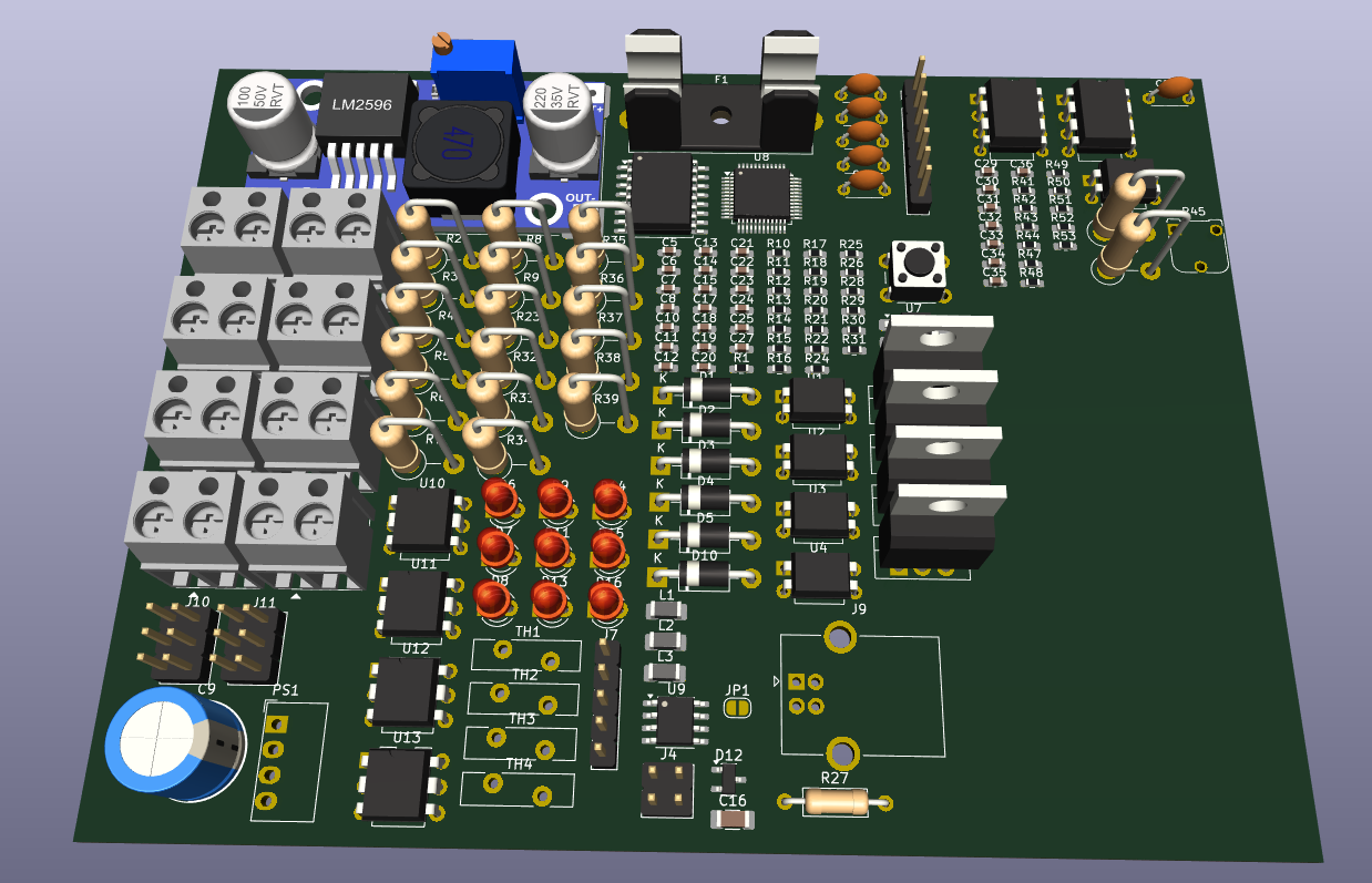
Here’s the board assembled in FreeCad:
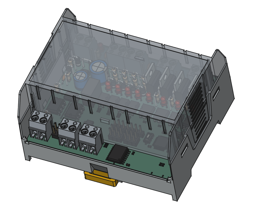
I’m really happy with how the product is turning out. I’ll make the label for it later as well.
I just need to move the connectors a bit away from the wall; they’re too close, which could cause assembly interference.
Next post I will make these corrections as well.
If you have any questions or recommendations, feel free to contact me via email.